Semiconductor technology: Turning India’s dream to reality
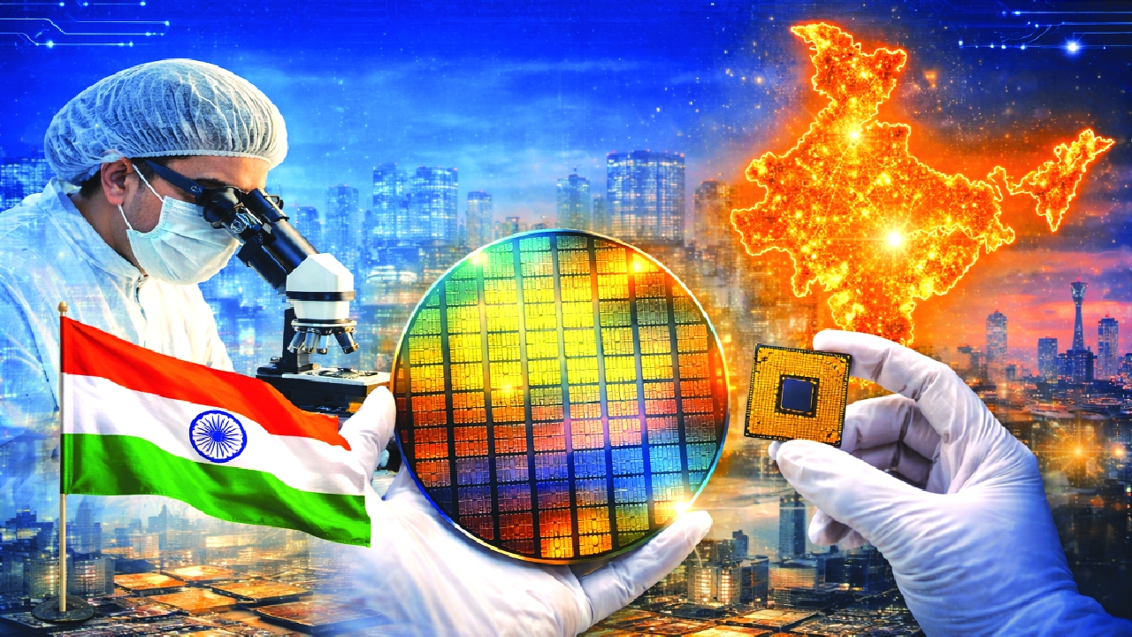
India, a remarkable country in this planet due to rich natural source of raw materials such as chemicals, rare earth minerals, and gases, which is the need of the hour for the semiconductor supply chain. India is the powerhouse of semiconductor transformation from Indian soil to silica and finally finished System on Chip [SoC]: VIKRAM 3201, SHAKTI Processors which are “Vocal for Local Indian Swadeshi semiconductor chips.”
Global surge in advanced technologies urge India to become self-reliant in advanced semiconductor technologies. India established itself as a strong service nation for centuries. Although India has strong IT foundation, butour nation swiftly and safelymakes an equivalent shift to a promising future by building
a focused hardware base. It has pushed and crossed several boundaries of valley of death curve to build Swadeshi and Vocal for Local products in semiconductor technologies.
India’s Karma Bhoomi is a land of fertile semiconductor valleys. Semiconductor valleys spread across each corner of our nation. The growing demand of chips
in potential applications like power/energy (smart energy meters), automotive industry, critical healthcare applications, smart and precession farming, smart cities, aerospace, and telecommunication industry pushes India to
the verge of establishing niche technologies in homeland thereby to meet the demand supply ecosystems of semiconductor chips across the globe. India is making a big breakthrough to advance world’s famous Moore’s law through working on next generation iconic 2D materials like Graphene with 3D integrationarchitecture thereby achieving
More than Moorephilosophy. To realise this dream to reality, Indian industry leader, Larsen & Toubro Semiconductor Technologies is establishing India’s first 2D innovation hub in collaboration with Indian Institute of Science [IISc], Bangalore to develop deep-scale wafer fabrication, prototype, and capacity building program. India has established first Centre of Excellence and innovation
hub for 2D material — Graphene in Kerala which will boost the semiconductor research and innovation in 2D materials leading to achieve the Make in India Mantra throughoptimising Man, Machine, Material, and Money.
Global partners like Micron, Foxconn, Qualcomm, IBM, Intel, Google, Microsoft, Applied Materials, Texas Instruments and NVIDIA see a huge and rapid market growth for semiconductor chips in India and across the entire world. The best example for our nation is Texas instrumentswhich has strong link in Indian market for more than decades in electronic design systems.
The advent of Government of India’s revolutionary schemes like production linked incentives and design linked incentives give a ‘good push’ for employment linked incentives. India establishes a strong connect between the design of chips from classroom to clean room. Semiconductor technology has travelled a spectacular journey from Indian classroom to clean room chip fabrication.
Hon’ble Prime Minister of India Shri Narendra Modi vision towards the Viksit Bharat@2047 has paved the way for global partners like Micron to launch the semiconductor assembly, testing, marking, and packaging of semiconductor devices in Sanand, Gujarat. Hon’ble Union Ministerof Railways, Ministry of Information and Broadcasting, and Ministry of Electronics & Information Technology, Government of India Shri Ashwini Vaishnaw had mentioned that “just imagine, writing the entire Ramcharitmanas on the nail of this thumb and entire book is like making a semiconductor.”
This example reflects the significance of high precision, resolution, accuracy, sensitivity, and meticulous committed preparations by utilising advanced emerging nanoimprint lithography technologies deployed in Indian institutions and industries which is required for semiconductor fabrication, manufacturing, and advanced characterisation tools and techniques.
India has the clean room facilities and fabrication laboratories at Indian Institute of Science (IISc), Bangalore, Indian Institute of Technology, IIT Bombay and Nanoscale Research Facility at Indian Institute of Technology, IIT Delhi. India’s collaboration and partnership with Micron have established the pioneering world’s largest superpower Cleanroom facility aligning with global standards at the industrial set up in Gujarat, India.
Additionally, the India’s IT major HCL joined hands with Foxconn to lay the foundation stone of semiconductor chip manufacturing plant in Uttar Pradesh.
This proves the foreign investments and innovation ecosystems to build a strong digital transformation public infrastructure in India. India has stepped into the sparkling journey of establishing a large-scale scalable semiconductor unit to manufacture the DRAM and NAND chips in India.
And India has successfully designed the pioneering 2nm chip in collaboration with Qualcomm addressing the gap of design and deployment. Indian education ecosystems boost the semiconductor technologyMinistry of Electronics and Information Technology, Government of India strengthened higher education institutions across India with world-class Electronic Design and Automation tools world-class Electronic Design Automation (EDA) being supported by global semiconductor simulation tool giants like Synopsys, Cadence, Siemens, Renesas, Ansys and AMD.
Ministry of Skill Development and Entrepreneurship, Govt. of India pushes National Educational Policy 2020 which has enabled differentOn-the-Job Training (OJT) demand programsacross higher educational institutions like apprenticeship enabled degree/diploma programs, research based AICTE internships, community-based learning like MY Bharat, virtual labs, to build a strong talent pool in India thereby meet the growing demands for semiconductor job market.
Government of India under the flagship initiative of The Ministry of Tribal Affairs (MoTA) in collaboration with CeNSE Indian Institute of Science, IISc, Bangalore is building a nationwide capacity building training program specially crafted for tribal students.
It is aNational Skill Qualification Framework (NSQF) certified semiconductor training program which has interesting features of both theory and firsthandcourses of 60-hour and 90-hour foundation and advanced online and offline courses, respectively. These courses will train and empower the tribal students. Indian Institute of Science (IISc), Bangalore in collaboration with Synopsis and Samsung is
offering Cohort training/fellowship program under India Semiconductor Workforce Development Program for undergraduate engineering and science students.
This program honesthe skills of young talent pool thereby making them Semiconductor Ready for our nation. NXP’s Women in Tech program (WIT) focuses women on developing skills on semiconductor design. These are a nation building exercise for developing nanofabrication skills leading to meet the demands of semiconductor manufacturing industry in India and across the globe.
India’s homegrown advanced design and fabrication laboratory named as semiconductor laboratory at Mohali, Chandigarh under Ministry of Electronics and Information Technology, Govt. of India has built India’s first chip called Vikram 3201 in collaboration with Indian Space Research Organization, ISRO Bangalore. It offers research internships to project based learning for students across the nation.
The pioneering schemes of Chips to Startup (C2S) under Ministry of Electronics and Information Technology, Govt. of India has established advanced chip design labs across higher educational institution is a boon to build semiconductor talents across each corner of our nation. The cohort training program offered under the C2S enables the faculty member to train the students to design chips starting from university labs to shop floors in manufacturing plants. The flagship programs under Centre for Development of Advanced Computing, C-DAC, National Institute for Electronics and Information Technology, NIELIT has enabled young minds to reskill and upskill in semiconductor design.
Ministry of Education, Government of India under National Mission on Education through Information and Communication Technology (ICT) has successfully launched a Free/Libre and Open-Source Software for Education called as FOSSEE in collaboration with Indian Institute of Technology, IIT Bombay. This is a project-based semiconductor program that provides free access to open-source tools like eSim, Scilab, FreeCAD and many more for students and faculty members and promotes the use of FLOSS tools in academia and research.
i-STEM which is pioneering network of platform established under Office of Principal Scientific Advisor, Government of India provides free access to reach to nearby institutions which has in-house advanced experimental facilities knockevery corner of the nation.
Government of Karnataka has established a collaboration partnership with IESA (India Electronics and Semiconductor Association) to form the Semiconductor Fabless Accelerator Lab which is first of its kind Centre’s of Excellence focused on building young startups to design and develop semiconductor products including the IP ecosystems and semiconductor tapeouts. Higher Educational Institutions like Dayalbagh Educational Institute (Deemed University), Agra and institutions across the nation are establishing Fab labs to boost the design, fabrication and prototypes thereby pushing the startup ecosystems.
India’s Way forward for semiconductor technologies
India’s tradition old pride ancient historicdesign symbols such as the spinning wheel (charkha), the lotus, Buy Swadeshi and Bharat Mata (Mother India), instill India’s cultural and design heritage foundations. India boosts the evolution and revolution of design education in establishing a National Institute of Design [NID] in the Northeastern region to inculcate the design and creative skills among the students of our nation. National Research Development Corporation, under Department of Scientific and Industrial Research, Ministry of Science and Technology, Government of India and Ministry of Micro Small and Medium Enterprises, Government of India has established Design Cline center to facilitate and promote the design of products and services.
Indian talents are designing and building the pioneering breakthrough semiconductor chips starting from pacemaker in healthcare applications to intelligent automotive industry in the C2S centers across the nation. India’s focused vision for Make in India and Market in India and across the globe enabled semiconductor chips and products available in MSMEs Government to Market Place portal (GeM).
Global countries have established a deep partnership and alliances with India because of its robust policy framework and strong vision like”Sabka Saath, Sabka Vikas, Sabka Vishwas, Sabka Prayaas” to build an Aatmanirbhar Bharat. Our nation has transformed bare lands into treasures in the present decade through establishing Digital Experience Zone, innovation hubs,Centre’s of excellence, advanced manufacturing plants, and most importantly capacity building of youth through skill mission. Additionally, India’s ease of doing business with global countries has earmarked our nation to be the market leader in semiconductor technologies and allied domains like Artificial Intelligence. Indian scientists are aiming to develop ‘angstrom-scale’ chips to break the emerging value chain proposition of chip designs. This will steadily and strongly make India to travel towards Amrit Kaal. UN has designated year 2026 as International Year of Volunteers. India has a strong belief to build a huge young volunteer base in semiconductor technologies to achieve the Viksit Bharat@2047.
India reverberates the powerful message of Hon’ble Prime Minister of India Shri Narendra Modi that “India is ready, India is reliable, and India delivers”which echoes to the entire world.
Writer is a Head Institute Industry Interface Program Hindustan College of Science and Technology, Mathura; views are personal